The Rabbit 2000 processor was designed as a clone of the popular Zilog Z180 processor, but with expanded capabilities. It is both a powerful and inexpensive processor, designed for embedded systems use. It has a total of 80 pins, with 20 lines used as address bus and an 8 lines used as the data bus. Other pins are used to connect to various external components. Some of the pins are used for accessing RAM and ROM, while others are used as interrupt signals or slave processor control pins.
The Rabbit 2000 requires two crystals in order to operate. The main crystal is used to run the Rabbit at a wide range of speeds, ranging from 1.8 MHz up to 30 MHz, depending on the oscillation frequency of the crystal used. The Rabbit can also double the crystal clock to run twice as fast, although the overall maximum speed the processor supports is about 30 MHz. It also supports dividing the clock by a factor of 8, which provides for reduced power usage. Yes, the processor can both double and divide by 8 for divide by 4 operations also. The second crystal must oscillate at 32 KHz, which is used mainly for running the real-time clock at a known, fixed frequency. The processor can be operated by the 32 KHz clock, in which case the main crystal is powered down, for an ultra low power mode. In this mode the processor itself may only use about 25 ?A of current and much of the external circuitry, like the high frequency clock is turned off. It is capable of being run using 5, 3.3 or 2.7-volt power sources, although high frequency operations normally require the higher voltage supplies.
The Rabbit processor supports at least 1 MB of memory directly and can even go beyond this by using some of its parallel port lines as chip select lines. It has built-in support for using both static RAM and flash RAM. Most memory devices can be directly connected to the Rabbit data and address bus, without needing any additional buffering or control chips. This is called glueless chip technology. It saves money by eliminating the chips needed to act as buffers between the processor and RAM chips in many other designs.
When it comes to input and output the Rabbit really shines. It has total of 40 I/O pins that are normally used as 5 parallel ports. Some of the parallel ports can be reconfigured to operate as serial ports, which compliment the included 4, dedicated serial ports. Each serial port can operate at a wide range of baud settings, with 7, 8 and 9-bit protocol support. Serial ports A and B can also be operated in synchronous mode. One of the ports can even be setup to interconnect two Rabbit processors together with one acting as a master unit and the other a slave. Internally, the Rabbit has 2 general-purpose timer registers, a separate watchdog timer and a 48-bit wide real time clock for precise time requirements.
The Rabbit is designed to easily support downloading and storing programs in memory. A very short program stored in internal ROM scans a special programming port upon reset or power up. This bit of code reads 3 bytes of data from the port in each pass. The first two bytes received form an address that the third byte is saved to. Once the values 0x80, 0x24, and 0x80 are received, the ROM routine exits and the processor runs the code found at memory location 0x0000. This first bit of code runs at 2400 baud always.
Normally, the code downloaded during the initial bootstrap is stored to memory location 0x0000. This section could be the entire program, but more likely it is a small helper program that switches the port into high-speed mode, 19.2 K to 115.2 K baud, and then downloads the real program and writes it into Flash RAM. There are many ways to implement the bootstrap, but generally the code will be downloaded and stored in the Flash RAM. Later when the unit is powered up, without the programming cable being attached, the processor will immediately execute the program stored in the Flash RAM chips. This is the normal mode of operation when this processor is used in an embedded system.
This processor has a large number of internal registers. There are sixteen 8-bit registers called A, B, C, D, E, F, H and L. The other eight registers are known as A', B', C', D', E', F', H' and L'. All the secondary registers can be swapped quickly with the primary registers and are very useful for holding temporary values. The F register is a flags register than cannot be directly modified. Instead it is used to store status information about the last instruction that was executed. For example, when subtracting a number from the A register, the 'zero' bit in the flag register will be set if A is equal to zero after the operation completes.
Two 8-bit registers can be combined to form a 16-bit wide register. Pairing is done as AF, BC, DE and HL. There are also 4 general-purpose 16-bit registers called IX, IY, SP and PC. IX and IY are designed for usage as an index to data arrays mostly. The SP register is used to control the stack pointer and the PC register tracks program execution.
There are also 4 extra registers designed for special purposes. The IP register gives the programmer the ability to assign priorities to interrupts. Two bits are used for each interrupt, for a total of 4 different priority levels. The IIR and EIR registers are used for internal and external interrupt handling.
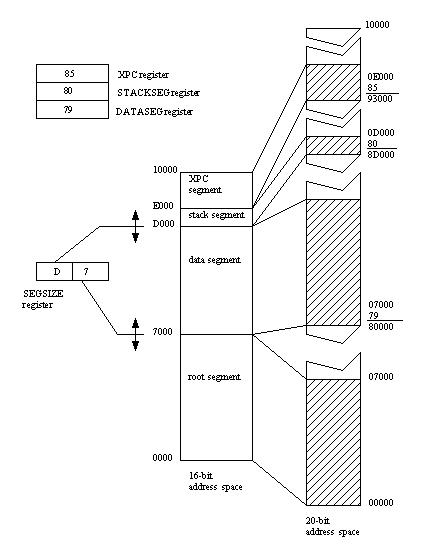
Lastly, there are 3 registers that are used to combine with 16-bit addresses to form full 24-bit addresses. The DATASEG and STACKSEG registers hold a special value that indicates where in memory the data and stack segments are located. Each segment is limited to accessing 64KB of data at any given moment, but the segment registers can be changed as needed to access all memory available. Generally, most software will not need more than 64KB of combined data and stack space. If it is needed, then the programmer must take special steps to address memory beyond this.
On the other hand, exceeding 64KB of program code is quite common. For this reason, the processor also includes one additional segment register called the XPC register. This register is used to setup a sliding window in a special 8K region of memory. Normally the XPC and PC registers combine to form the real 24-bit address of the next instruction to be executed. If the processor notices that the PC register ever gets close to the end of the 8K window, the XPC register is automatically adjusted to point to the next 4K block of code in flash or static RAM. This technique is known as memory mapping and we will discuss it in more detail below.
Memory usage in the Rabbit 2000 is similar to the way the original Z80 used memory, with a couple of very important enhancements. The Z80 used 16-bit addresses, which provide for up to 64K of memory. 16-bit addresses have a tremendous advantage over 32-bit addresses, since they use up half the space to store and use. 64K of memory is quite limiting however, so the Rabbit actually supports 24-bit wide addresses. This allows the processor to use up to 1 MB of memory, without needing any extra support chips.
In order to use all this memory however, a 16-bit address must be combined with a special 8-bit segment address to create a true 24-bit address. Since the XPC address area is 8K in size, all functions that are downloaded to the Rabbit must fit within an 8K block. More than one function may occur in the 8K block, and if this happens, then only 16-bit addresses are used to call or jump to routines in the same 8K block. When calling functions that are outside the current 8K block, a new XPC segment must be loaded to switch to the new 8K block where the function resides. Luckily for us, the compiler will track and handle this automatically. The net result is that the Rabbit can handle a program of up to 1 MB in size and still have almost 64K of data available for variables and such. Please note that constants, like error message strings, are normally stored in the same area as the code, so as to not waste the 64K of data area.
While this may seem strange at first, it is the same technique that has been successfully used for years in other processors like the 8088, Z80, 80186, and even their bigger, faster cousins the 80286, 80386, and Pentium, when operating in real mode. Of course, the bigger processors like the Pentium also support a mode of operation where everything is 32-bit wide, which allows accessing up to 4GB of RAM. This is overkill for most embedded systems and the Rabbit's design is much cheaper overall and normally does not limit its usefulness.
The parallel ports A through E are available as 8-bit wide data registers. Most of the ports bits can be used as either input or output pins, depending on the setting in a control register. The parallel port registers are as follows:
| Port | Data Register | Control Register(s) | Comments |
|---|---|---|---|
| A | 0x30 (R/W) | 0x24 | Also acts as a slave/programming port. |
| B | 0x40 (R/W) | N/A | Bits 6 & 7 are output only, Bits 0-5 are input only. The pins in this port are used as clock signals when serial ports are configured for synchronous operations. Some of these pins are also used when a slave processor is connected to a master. |
| C | 0x50 (R/W) | 0x55 | Bits 0,2,4 & 6 are output only; Bits 1,3,5, & 7 are input only. If the processor is reconfigured, these pins can also be used as serial input and output signals for serial ports A-D. |
| D | 0x60 0x68-0x6F bitmasks to pins 0 to 7 | 0x64, 0x65, 0x66, & 0x67 | This port can be used for input or output. In addition, the pins can be configured as high-low drive, or open-drain output, which is useful for scanning keys aligned in rows and columns. Bits 4-7 can also be reconfigured as serial port A and B transmit/receive pins, if needed. |
| E | 0x70 0x78-0x7F bitmasks to pins 0 to 7 | 0x74, 0x75, & 0x77 | This port can be used for input or output. They can also be reconfigured to act as external I/O control signals too. This mode is often used when connecting as master and slave processors together. |
There are four serial ports available as 8-bit wide data registers. The serial ports can be operated at speeds of up to 1/32 of the main clock frequency, when used in an asynchronous mode. When used in synchronous mode, the ports can be operated at up to ¼ of the main clock frequency. Each has an associated status register that is used to control serial data input and output timing. The serial port registers are as follows:
| Port | Data Register | Status Register | Control Register(s) | Comments |
|---|---|---|---|---|
| A | 0xC0 | 0xC3 | 0xC1 & 0xC4 | |
| B | 0xD0 | 0xD3 | 0xD1 & 0xD4 | |
| C | 0xE0 | 0xE3 | 0xE1 & 0xE4 | Uses parallel port C's pins when configured to operate serially. |
| D | 0xF0 | 0xF3 | 0xF1 & 0xF4 | Uses parallel port D's pins when configured to operate serially. |
The Rabbit 2000 processor also has two general-purpose timer registers. Timer A is normally used as clock generators for the serial ports, while Timer B is normally available for any other timing operations needed.
Timer A is really 4 different timers in one that support creating up to 4 different baud rate settings, one for each serial port, by loading a divisor constant into a control register. The peripheral clock divided by 2 is connected as the input to the timer. As each clock pulse is received, the timer compares the current clock count to a constant value, one for each of 5 different registers. If the count in a counter register matches the value stored in the corresponding constant register, the timer then generates an interrupt. This interrupt signals the CPU which then knows that the time is correct for sending or receiving additional data via the serial port. The Rabbit processor supports 3 different interrupt priorities and the timer can be setup to generate interrupts with priority 1, 2 or 3. Please note that if you do not need serial communications, you can use the interrupts to act as signals for any kind of periodic processing.
Timer B on the other hand can be used for any purpose desired. It uses a 10-bit wide count and 2 10-bit wide match registers to allow for longer timing intervals. This is done by combining 8 bits from one register with 2 more bits from a second register for both the counting and matching registers. Timer B also generates an interrupt, configurable for priorities 1, 2 or 3, whenever the count register matches one of the match registers. Timer B can be driven from the same peripheral clock divided by 2 as Timer A, or it can be driven by the peripheral clock divided by 16, or it can be driven by Timer A's output.
| Timer | Constant/Match/Divisor Registers | Control/Status Registers | Comments |
|---|---|---|---|
| A | 0xA3, 0xA9, 0xAB, 0xAD, 0xAF | 0xA0, 0xA4 | Register 0xA3 sets the main divisor, while 0xA9, 0xAB, 0xAD and 0xAF control timer outputs A4 (Serial A), A5 (Serial B), A6 (Serial C) and A7 (Serial D) |
| B | 0xB2 & 0xB3 (WR), 0xB4 & 0xB5 (WR), 0xBE & 0xBF (RD) | 0xB0, 0xB1 | 0xB2 (2 bits) and 0xB3 make match/divisor register B1 0xB4 (2 bits) and 0xB4 make match/divisor register B2 0xBE (2 bits) and 0xBF hold the current Timer B count |
The Rabbit 2000 processor also has a real-time clock that can be used for more precise timing operations. This clock is a free-running 48-bit counter, which makes it large enough to count up for about 100 years. The 32 KHz clock always drives the real-time clock. If the backup battery is installed, the real-time clock continues to run when main power is removed. It can be reset to zero or disabled if not needed.
| RTC Count Registers | RTC Control Register | Comments |
|---|---|---|
| 0x02, 0x03, 0x04, 0x05, 0x06, & 0x07 | 0x01 | Before reading the count registers, you must first write a value (any value) to register 0x02. This updates all the other registers with the current RTC count, which you can then read from register 0x02 to 0x07. |
The Rabbit 2000 processor has one additional timer we must discuss. It is called the watchdog timer and its purpose is to detect when the current program has locked up or crashed. When enabled, the processor periodically checks the watchdog timer to determine if it matches a timeout value. If the watchdog timer does reach this value, the processor assumes the program has crashed or locked up in some way and the processor resets itself, which has the effect of doing a reboot. The program that is running is responsible for periodically resetting the watchdog timer before the timeout is reached. The timeout can be programmed to occur in 2, 1, 0.5 or 0.25 seconds, depending on the needs of the application.
| Register | Comments |
|---|---|
| 0x08 (WDTCR) | Programs the timeout setting. 5Ah = 2 second 57h = 1 second 59h = 0.5 second 53h = 0.25 second Other values are ignored. |
| 0x09 (WDTTR) | Select the clock used to drive the Wtd. 51h = LSB clocked by peripheral clock 52h = MSB clocked by peripheral clock 53h = MSB and LSB clocked by peripheral clock 54h = Disable WDT (Must be proceeded by 51h, 52h or 53h first) Other values = Normal (clock using 32KHz clock) |
| Pin Group | Pin Name | Direction | Function | Pin Numbers |
|---|---|---|---|---|
| Hardware | CLK | Output | Peripheral clock output. This signal is derived internally from the main system oscillator as perclk, and may be divided by 8, doubled, or both, by programmable internal circuitry. This signal is enabled after reset. Under program control, this pin can output the full internal clock frequency, or 1/2 the internal frequency, or it can be used as a general-purpose output pin under software control. See also: Global Output Control Register (GOCR = 0x0E). | 1 |
| /RESET | Input | Master reset. | 37 | |
| XTALA1 | Input | Quartz crystal for 32 kHz clock oscillator. Lines to the crystal should be short and shielded from cross talk. If an external clock is used, the external clock should drive this pin. | 40 | |
| XTALA2 | Output | Quartz crystal for 32 kHz crystal oscillator. Do not connect if an external clock is used. | 41 | |
| XTALB1 | Input | Quartz crystal for main system oscillator. Lines to the crystal should be short and shielded from cross talk. If an external clock is used this pin should be driven by the external clock. | 90 | |
| XTALB2 | Output | Quartz crystal for main system oscillator. Do not connect if an external clock is used. | 91 | |
| CPU Buses | A0-A19 | Output | Address bus. | 7, 17-20, 61-68, 70-75, & 79 |
| D0-D7 | Bi-directional | Data bus. | 9-16 | |
| Status/ Control | /WDTOUT | Output | WDT timeout--outputs a pulse when the internal watchdog times out. May also be used to output a 30 µs pulse. | 34 |
| Status | STATUS | Output | Programmable for functions: 1. driven low on first opcode fetch cycle 2. driven low during interrupt acknowledge cycle 3. to serve as a general-purpose output. See also: Global Output Control Register (GOCR = 0x0E). | 38 |
| Status | SMODE1 SMODE0 | Input | Startup mode select (SMODE1 = pin 35, SMODE0 = pin 36) to determine bootstrap procedure. (SMODE1 = 0, SMODE0 = 0) start executing at address zero. (0,1) cold boot from slave port. (1,0) cold boot from clocked serial port A. (1,1) cold boot from asynchronous serial port A at 2400 bps. The smode pins can be used as general input pins once the cold boot is complete. | 35-36 (1:0) |
| Chip Selects | /CS0 | Output | Memory Chip Select 0--connects directly to static memory chip select pin. Normally this pin is used to select base flash memory that holds the program. | 8 |
| /CS1 | Output | Memory Chip Select1--normally this pin is connected directly to static RAM chip select. /CS1 can be optionally forced continuously low under software control, a feature that aids in the use of battery-backed RAM when the chip select must pass through a controller that may have a slow propagation time. | 5 | |
| /CS2 | Output | Memory Chip Select 2--connect to static memory chip. Use this chip select last. | 4 | |
| Output Enables | /OE0 | Output | Memory Output Enable 0--connect directly to static memory chip. | 6 |
| /OE1 | Output | Memory Output Enable 1--alternate memory output enable allows chip selects to be shared between two memory chips. | 76 | |
| Write Enables | /WE0 | Output | Memory Write Enable 0--connect directly to static memory chip. This pin may be disabled under software control to write protect the chip. | 69 |
| /WE1 | Output | Memory Write Enable 1--connect directly to static memory chip. This pin may be disabled under software control to write protect the chip. | 80 | |
| I/O Control | /BUFEN | Output | I/O Buffer Enable--this signal is driven low during an external I/O cycle and may be used to control 3-state enable on the bus buffer. The purpose is to save power by not driving the I/O address or data lines on every bus cycle. | 33 |
| I/O Read Strobe | /IORD | Output | I/O read strobe. Driven low on an external I/O read bus cycle. May be used to drive glue logic concerned with I/O expansion, such as the direction pin on a bidirectional bus buffer. See also programmable strobes in port E. | 32 |
| I/O Write Strobe | /IOWR | Output | I/O write strobe. Driven low as a write strobe during external I/O write cycles. Is enabled by the I/O bank control register. See also programmable strobes in port E. | 31 |
| I/O Port A | PA0-PA7 | Input/ Output | These 8 bits serve as general-purpose input output or they serve as the data port for the slave port. On reset these pins are set to inputs and they float. | 81-88 |
| I/O Port B | PB0-PB7 | 6 In/2 Out | I/O Port B. When used as parallel I/O, PB7 and PB6 are outputs only. PB0-PB5 are inputs only. PB0 and PB1 can be outputs when set up as the clock for the clocked serial ports. On reset, the outputs are set to zero. If the slave port is enabled, the following alternate assignments apply: PB7--/SLAVEATTN: slave requests attention. PB5, PB4--address lines (SA1, SA0) for slave registers. PB3--slave negative write strobe from master. PB2--slave negative read strobe from master. If serial port A is enabled in clocked mode, then PB1 is the bi-directional clock line. If serial port B is enabled in clocked mode, then PB0 is the bi-directional clock line. | 93-100 |
| I/O Port C | PC0-PC7 | 4 In/4 Out | I/O Port C. When used as a parallel port, bits 1, 3, 5, 7 are inputs and bits 0, 2, 4, 6 are outputs. Bits 0, 2, 4, 6 can alternately be selectively enabled to serve as the serial data output for serial ports D, C, B, and A respectively. Bits 1, 3, 5, 7 serve as the serial data inputs for serial ports D, C, B, and A. These inputs can also be read from the parallel port register when they are being used by the serial port UART. | 51, 54-60 |
| I/O Port D | PD0-PD7 | Input/ Output/ output open drain | I/O Port D. Each bit may be individually selected to be an input or output. Each output may be selected to be high-low drive or open drain. Outputs are buffered by timer-synchronizable registers for precision edge control. PD6 can be programmed to be an optional serial output for serial port A. PD4 can be programmed to be an optional serial output for serial port B. PD7 and PD5 can be used as alternate serial inputs by serial ports A and B, in which case these pins should be programmed as inputs. | 43-50 |
| I/O Port E | PE7-PE0 | Input/ Output | I/O Port E. Each bit may be individually selected to be an input or output. Outputs are buffered by timer-synchronizable registers for precision edge control. Each of the port lines can be individually selected to be an I/O control signal instead of a parallel I/O line. Each of the 8 possible I/O control signals is a strobe energized on an external I/O cycle to 1/8th of the 64K external I/O space. Each strobe can be programmed to be a chip select, a write strobe, a read strobe or a combined read and write strobe. Any port bit used as an I/O control strobe must be programmed as an output bit. If the slave port is enabled, PE7 is used as the slave register chip select signal (negative active). PE7 should be programmed as an input for the slave register chip select function to work. If PE7 is programmed as an output and set low, then the slave register chip select will always be activated. PE0 and PE4 serve as alternate inputs for external interrupt 0. PE1 and PE5 serve as alternate inputs for external interrupt 1. If PE0 is enabled, then PE1 must also be enabled and similarly for PE4 and PE5. The interrupt is triggered in software on fall, rising or both edges. If both interrupts are enabled, they are or'ed together after edge detection has been performed on each input individually. The port bits must be set up as inputs for the to use them as interrupt request inputs. | 21-26, 29, 30 |
| Power | VBAT | N/A | +3.0 V (battery backup), +3.3 V or +5.0 V | 42 |
| VDD | N/A | +3.3 V or +5.0 V | 3, 28, 53, 78, & 92 | |
| VSS | N/A | Ground | 2, 27, 39, 52, 77, & 89 | |
| Serial Ports | CLKA | Input/ Output | Clock for serial port A when operating in synchronous mode. Alternate assignment for PB1. | 94 |
| CLKB | Input/ Output | Clock for serial port B when operating in synchronous mode. Alternate assignment for PB0. | 93 | |
| RXA, TXA, RXB, TXB, RXC, TXC, RXD, & TXD | RX--input TX--output | Serial inputs and output for serial ports A-D. These are alternate pin assignments for parallel port C. | 51, 54-60 | |
| ARXA, ATXA, ARXB, & ATXB | RX--input TX--output | Alternate serial inputs and output for serial ports A and B. These are alternate pin assignments for parallel port D, PD4-PD7. | 43-46 | |
| Slave Port | SD0-SD7 | Bidirectional | Slave port data bus. An alternate assignment for parallel port A. | 81-88 |
| /SLAVEATTN | Output | /SLAVEATTN--Slave is requesting attention from the master. An alternate pin assignment for parallel port B, bit 7. | 100 | |
| /SRD | Input | Strobe used to read one of the slave registers. An alternate pin assignment for parallel port B, bit 3. | 96 | |
| /SWR | Input | Strobe used to write a slave register. An alternate pin assignment for parallel port B, bit 2. | 95 | |
| SA0, SA1 | Input | Address lines to address slave registers. An alternate pin assignment for parallel port B, bits 4 and 5. | 97,98 | |
| /SCS | Input | Chip select for slave port, active low. An alternate pin assignment for parallel port E, bit 7. | 21 | |
| I/O Strobes | /I0,/I1, /I2,/I3, /I4, /I5, /I6, & /I7 | Outputs | I/O strobes. Each strobe uses 1/8th of the I/O space or 8K addresses. Each strobe can be programmed as: chip select, read, write, combined read or write. These are alternate pin assignment for parallel port E, bits 0-7. Each pin may be individually re-assigned from parallel port to strobe functionality. | 21-26, 29, 30 |
| External Interrupt 0 | INT0A, INT0B | Inputs | These pins are sampled and an interrupt request for external interrupt number 0 is latched on a specified transition (pos, neg, either). There is a separate latch for each pin. May be enabled when this pin is set up as input for parallel port E. The value of the pin may also be read via the parallel port. Uses bits 0, 1 of the parallel port. If parallel port is set up as output, the parallel port output may be used to cause the interrupt. | 24, 30 |
| External Interrupt 1 | INT1A, INT1B | Inputs | These pins are sampled and an interrupt request for external interrupt number 1 is latched on a specified transition (pos, neg, either). There is a separate latch for each pin. May be enabled when this pin is set up as input for parallel port E. The value of the pin may also be read via the parallel port. Uses bits 4, 5 of the parallel port. If parallel port is set up as output, the parallel port output may be used to cause the interrupt. | 23, 29 |
| Address | Reset Value | Functionality |
|---|---|---|
| Global Control Status Register | ||
| GCSR=00h | 11000000 | Controls clocks, periodic interrupts, and monitoring of watchdog. |
| Real-Time Clock (RTC) Registers | ||
| RTCCR=01h | 00000000 | RTC Control Register. |
| RTC0R=02h | xxxxxxxx | RTC Byte 0 Register. |
| RTC1R=03h | xxxxxxxx | RTC Byte 1 Register. |
| RTC2R=04h | xxxxxxxx | RTC Byte 2 Register. |
| RTC3R=05h | xxxxxxxx | RTC Byte 3 Register. |
| RTC4R=06h | xxxxxxxx | RTC Byte 4 Register. |
| RTC5R=07h | xxxxxxxx | RTC Byte 5 Register. |
| Watchdog Timer Registers | ||
| WDTCR=08h | 00000000 | Control Register. |
| WDTTR=09h | 00000000 | Test Register. |
| Clock Control Registers | ||
| GOCR=0Eh | 00000x00 | Global Output Control Register. |
| GCDR=0Fh | xxxxx000 | Global Clock Doubler Register. |
| Memory Management Registers | ||
| MMIDR=10h | xxx00000 | Memory Management I and D Space Register. Controls I & D space enable and battery switchover support for /CS1. |
| XPC | 00000000 | Not an I/O register, but initialized to zero by reset. |
| STACKSEG=11h (Z180 CBR) | 00000000 | Stack segment memory pointer. Locates stack segment in physical memory. |
| DATASEG=12h (Z180 BBR) | 00000000 | Data segment memory pointer. Locates data segment in physical memory. |
| SEGSIZE=13h (Z180 CBAR) | 11111111 | Specifies start of data segment and start of stack segment in 64K memory space. |
| Memory Bank Registers | ||
| MB0CR=14h | 00000000 | Memory Bank 0 Control Register. Controls mapping of first memory quadrant 256K to physical memory chips. |
| MB1CR=15h | xxxxxxxx | Memory Bank 1 Control Register. Controls mapping of second memory quadrant to physical memory chips. |
| MB2CR=16h | xxxxxxxx | Memory Bank 2 Control Register. Controls mapping of third memory quadrant to physical memory chips. |
| MB3CR=17h | xxxxxxxx | Memory Bank 3 Control Register. Controls mapping of fourth memory quadrant to physical memory chips. |
| Slave Port Registers | ||
| SPD0R=20h | xxxxxxxx | Slave Port Register 0. Separate registers for read and write used for slave port communication. |
| SPD1R=21h | xxxxxxxx | Slave port register 1. |
| SPD2R=22h | xxxxxxxx | Slave port register 2. |
| SPSR=023h | 00000000 | Slave port status register. |
| SPCR=24h | 000x0000 | Slave port control register. |
| Parallel Port Registers | ||
| PADR=30h | xxxxxxxx | Parallel port A data register. R/W. |
| PBDR=40h | 00xxxxxx | Parallel port B data register. R/W. |
| PCDR=50h | x0x0x0x0 | Parallel port C data register. |
| PCFR=55h | x0x0x0x0 | Port C function register. |
| PDDR=60h | xxxxxxxx | Parallel port D data register. R/W. |
| PDCR=64h | xx00xx00 | Port D control register |
| PDFR=65h | xxxxxxxx | Port D function register. |
| PDDCR=66h | xxxxxxxx | Port D drive control register. |
| PDDDR=67h | 00000000 | Port D data direction register. |
| Port D Registers | ||
| PDB0R=68h | xxxxxxxx | Port D bit 0 register. W |
| PDB1R=69h | xxxxxxxx | Port D bit 1. |
| PDB2R=6Ah | xxxxxxxx | Port D bit 2. |
| PDB3R=6Bh | xxxxxxxx | Port D bit 3. |
| PDB4R=6Ch | xxxxxxxx | Port D bit 4. |
| PDB5R=6Dh | xxxxxxxx | Port D bit 5. |
| PDB6R=6Eh | xxxxxxxx | Port D bit 6. |
| PDB7R=6Fh | xxxxxxxx | Port D bit 7. |
| Port E Registers | ||
| PEDR=70h | xxxxxxxx | Parallel port E data register. R/W. |
| PECR=74h | xx00xx00 | Port E control register. |
| PEFR=75h | xxxxxxx | Port E function register. |
| PEDDR=77h | 0000000 | Port E data direction register. |
| PEB0R=78h | xxxxxxx | Port E bit 0 register. W |
| PEB1R=79h | xxxxxxx | Port E bit 1. |
| PEB2R=7Ah | xxxxxxx | Port E bit 2. |
| PEB3R=7Bh | xxxxxxx | Port E bit 3. |
| PEB4R=7Ch | xxxxxxx | Port E bit 4. |
| PEB5R=7Dh | xxxxxxx | Port E bit 5. |
| PEB6R=7Eh | xxxxxxx | Port E bit 6. |
| PEB7R=7FH | xxxxxxx | Port E bit 7 |
| External I/O Registers | ||
| IB0CR=80h | 00000xxx | External I/O control bank 0 |
| IB1CR=81h | 00000xxx | External I/O control bank 1 |
| IB2CR=82h | 00000xxx | External I/O control bank 2 |
| IB3CR=83h | 00000xxx | External I/O control bank 3 |
| IB4CR=84h | 00000xxx | External I/O control bank 4 |
| IB5CR=85h | 00000xxx | External I/O control bank 5 |
| IB6CR=86h | 00000xxx | External I/O control bank 6 |
| IB7CR=87h | 00000xxx | External I/O control bank 7 |
| External Interrupt Registers | ||
| I0CR=98h | xx000000 | External interrupt 0 control register. |
| I1CR=99h | xx000000 | External interrupt 1 control register. |
| Timer A Registers | ||
| TACSR=0A0h | 0000xx00 | Timer A Control/Status Register |
| TACR=0A4h | xxxxxxxx | Timer A Control Register |
| TAT1R=0A3h | 0000xx00 | Timer A1 Time Constant 1 Register |
| TAT4R=0A9h | xxxxxxxx | Timer A4 Time Constant 4 Register |
| TAT5R=0ABh | xxxxxxxx | Timer A5 Time Constant 5 Register |
| TAT6R=0ADh | xxxxxxxx | Timer A6 Time Constant 6 Register |
| TAT7R=0AFh | xxxxxxxx | Timer A7 Time Constant 7 Register |
| Timer B Registers | ||
| TBCSR=0B0h | xxxxx000 | Timer B Control/Status Register |
| TBCR=0B1h | xxxx0000 | Timer B Control Register |
| TBM1R=0B2h | xxxxxxxx | Timer B MSB 1 Reg |
| TBL1R=0B3h | xxxxxxxx | Timer B LSB 1 Reg |
| TBM2R=0B4h | xxxxxxxx | Timer B MSB 2 Reg |
| TBL2R=0B5h | xxxxxxxx | Timer B LSB 2 Reg |
| TBCMR=0BEh | xxxxxxxx | Timer B Count MSB Reg |
| TBCLR=0BFh | xxxxxxxx | Timer B Count LSB Reg |
| Serial Port A Registers | ||
| SADR=0C0h | xxxxxxxx | Serial port A data register receive/send. |
| SAAR=0C1h | xxxxxxxx | Serial port A alternate data register (transmit 9th bit) |
| SASR=0C3h | 0xx00000 | Serial port A status register. |
| SACR=0C4h | xx000000 | Serial port A control register. |
| Serial Port B Registers | ||
| SBDR=0D0h | xxxxxxxx | Serial port B data register receive/send. |
| SBAR=0D1h | xxxxxxxx | Serial port B alternate data register (transmit 9th bit) |
| SBSR=0D3h | 0xx00000 | Serial port B status register. |
| SBCR=0D4h | xx000000 | Serial port B control register. |
| Serial Port C Registers | ||
| SCDR=0E0h | xxxxxxxx | Serial port C data register receive/send. |
| SCAR=0E1h | xxxxxxxx | Serial port C alternate data register (transmit 9th bit) |
| SCSR=0E3h | 0xx00000 | Serial port C status register. |
| SCCR=0E4h | xx00x000 | Serial port C control register. |
| Serial Port D Registers | ||
| SDDR=0F0h | xxxxxxxx | Serial port D data register receive/send. |
| SDAR=0F1h | xxxxxxxx | Serial port D alternate data register (transmit 9th bit) |
| SDSR=0F3h | 0xx00000 | Serial port D status register. |
| SDCR=0F4h | xx00x000 | Serial port D control register. |